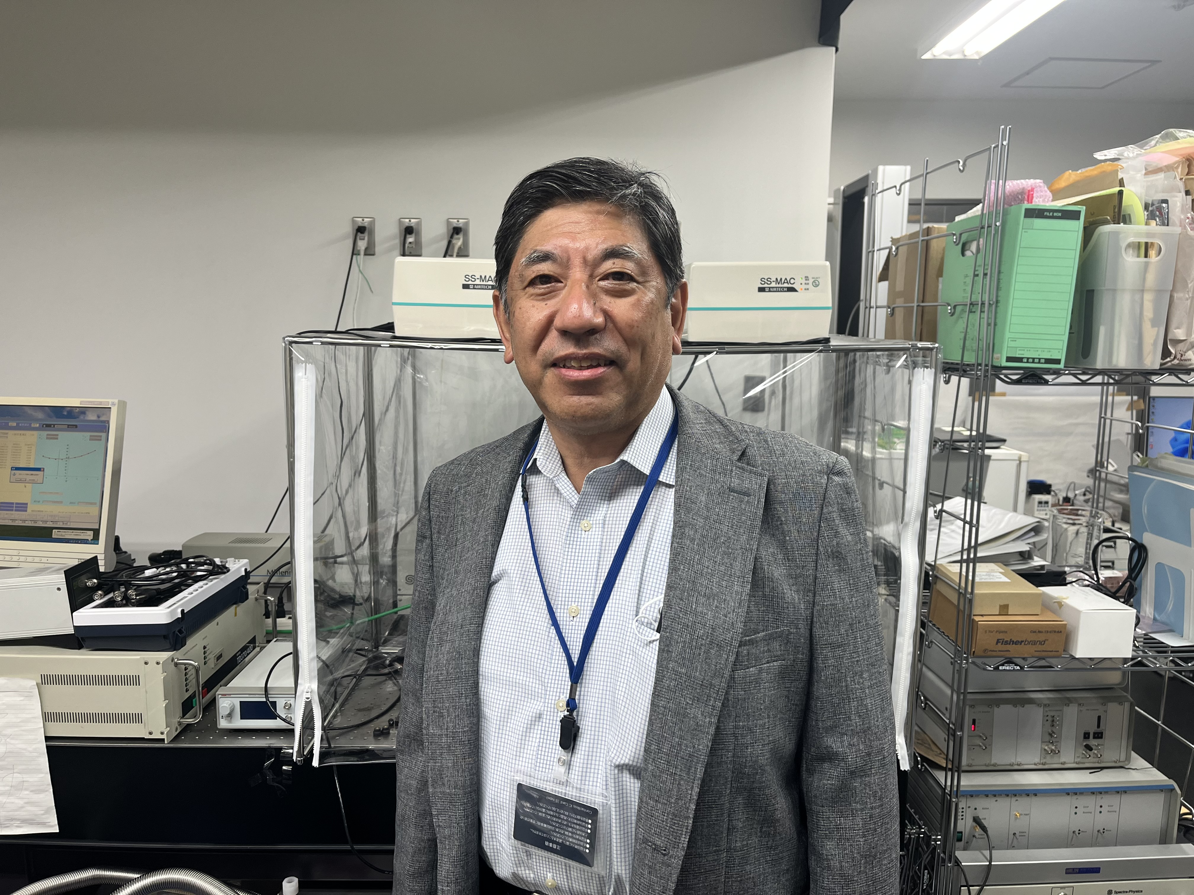
Profile
asufumi YAMADA
Guest Senior Researcher (Guest Professor)
mail
yyamada@aoni.waseda.jp
Career
Mar 1975 Graduated from Tokyo Toyama Public High School, Tokyou
Mar 1980 Bachelor of Science, Department of Applied Physics, Waseda Univ.
Mar 1982 Master of Science, Department of Physics and Applied Physics, Waseda Univ.
Oct 1990 Doctor of Engineering, Waseda Univ.
Job Experience
In 1982, Yasufumi Yamada joined the Electrical Communication Laboratories, Nippon Telegraph and Telephone Public Corporation (present NTT), Ibaraki, where he had been engaged in basic research on fabrication technologies on silica-based waveguide. This research leaded to essential optical components in optical communication network called planar lightwave circuits (PLC).
From 1987 to 1998, Dr. Yamada had been engaged in research and development on hybrid integration of opto-electric devices on a PLC platform.
In 1998, he transferred to NTT Electronics Corporation (NEL).
He first took on the challenge of launching a business on hybrid-integrated PLC (H-PLC),
From 2001 to 2005, he had been engaged in management of PLC fabrication factories.
From 2005 to 2011, he was Executive Manager of the PLC business division.
In 2011, he got promoted to Executive Director of NEL.
In 2014, he transferred to NEL crystal corporation which was a subsidiary of NEL, and he got promoted to President.
In 2019, he returned to NTT Electronics as Senior Adviser.
In March 2022, Dr. Yamada has retired NTT Electronics.
Awards
電子情報通信学会 論文賞および猪瀬賞(*)
(*)猪瀬賞; 論文賞を受賞した論文中の最優秀論文賞
受賞年月日 1998年5月
対象論文;
N. Uchida, Y. Yamada, Y. Hibino, Y. Suzuki, and N. Ishihara
"Low-Cost Hybrid WDM Module Consisting of a Spot-size Converted Laser Diode
and a Waveguide Photodiode on a PLC Platform for Access Nertwork System"
IECE Trans. Electron. Vol.E80-C (1997)88
Book
“Passive Micro-Optical Alignment Methods” (Taylor & Francis) 2005年発行
Chapter8 “Solder-Bump and Visual Alignment Technologies” pp.241-281
Major Papers;
<Paper>
(1) Y. Yamada, H. Terui, Y. Ohmori, M. Yamada, A. Himeno and M. Kobayashi
“Hybrid-integrated 4x4 optical gate matrix switch using silica-based optical waveguide and LD-array chips” J. Lightwave Technol. Vol.10 (1992) 383
(2) Y. Yamada, M. Yamada, H. and M. Kobayashi
“Optical Interconnections using a silica-based waveguide on a silicon substrate”
Opt. Engineer. Vol.28(1989)1281
(3) Y. Yamada and M. Kobayashi
“Single-mode optical fiber connection to high-silica waveguide with fiber guiding-groove” J. Lightwave Technol. Vol.LT-5 (1987) 1716
(4) Y. Yamada, M. Kawachi, M. Yasu and M. Kobayashi
“High-silica multimode channel waveguide structure for minimizing coupling loss”
J. Lightwave Technol. Vol.LT-4 (1986) 277
<Letter>
(5) Y. Yamada, S. Suzuki, K. Moriwaki, Y. Hibino, Y. Tohmori, Y. Akatsu, Y. Nakasuga, T. Hashimoto, H. Terui, M. Yanagisawa, Y. Inoue, Y. Akahori and R. Nagase
“Application of planar lightwave circuit platform to hybrid integrated optical WDM transmitter/receiver module” Electron. Lett. Vol.31 (1995) 1366
(6) Y. Yamada, A. Sugita, K. Moriwaki, I. Ogawa and T. Hashimoto
“An application of a silica-on-terraced silicon platform to hybrid Mach-Zehnder interferometric circuit consisting of silica-waveguide and LiNbO3 phase-shifters”
IEEE Photon. Tchnol. Lett., vol.6 (1994) 822
(7) Y. Yamada, A. Takagi, I. Ogawa, M. Kawachi and M. Kobayashi
“Silica-based optical waveguide on terraced silicon substrate as hybrid integration platform” Electron. Lett. Vol.29(1993) 444
(8) Y. Yamada, F. Hanawa, T. Kitoh and T. Maruno
“Low-loss and stable fiber-to-waveguide connection utilizing UV curable adhesive”
IEEE Photon. Technol. Lett., vol4 (1992)906
(9) Y. Yamada, Y. Ohmori, M. Yamada, H. Terui and M. Kobayashi
“Effect of waveguide facet reflection on hybrid-integrated optical gate switch”
Trans. IECE Japan, volE72 (1989) 282
(10) Y. Yamada, M. Kawachi, M. Yasu and M. Kobayashi
“Carbon-dioxide laser processing of porous glass layer for optical waveguide”
Appl. Opt. vol.24 (1985) 454
(11) Y. Yamada, M. Kawachi, M. Yasu and M. Kobayashi
“Fabrication of a high silica glass waveguide optical accessor”
Electron. Lett. Vol.20 (1984) 589
(12) Y. Yamada, M. Kawachi, M. Yasu and M. Kobayashi
“Optical fiber coupling to high-silica glass channel waveguide with fiber guiding groove” Electron. Lett. Vol.20 (1984) 313
Major Conference
<Invited>
(1) Y. Yamada “OE-device hybrid integration using PLC platform”
LEOS'97 ThB3 (1997)
(2) M. Yanagisawa and Y. Yamada
“Optical transceiver modules using PLC platform” CLEO/Pacific rim FT1 (1997)
(3) Y. Yamada “Hybrid integration with PLC and semiconductor devices” OECC'97 10D4-1 (1997)
(4) Y. Yamada “Optical hybrid integration technology using a PLC platform and spot-size converted devices” IPR'96 IThD1(1996)
(5) Y. Yamada “Hybrid optoelectronic integration with PLC platform” OECC'96 6A1-5 (1996)

